| Parent directory/ | - | - |
| 16 Tips for Using PCB Layout Software.pdf | 960.3 KiB | 2022-Jan-28 17:07 |
| A Lesson on PCB routing.pdf | 165.5 KiB | 2023-Sep-29 19:17 |
| A lesson on proper routing of PCBs.pdf | 165.5 KiB | 2022-Nov-22 18:18 |
| ADC PCB Layout - The reference path.mht | 1.6 MiB | 2014-Aug-11 11:51 |
| ANSI PCB Track Width Calculator.mht | 39.3 KiB | 2015-May-29 15:12 |
| Analysis of Board Layout to Help Cure Jitter Problems.pdf | 223.2 KiB | 2010-Jan-07 23:35 |
| Avoiding RF Oscillation.pdf | 599.8 KiB | 2022-Sep-25 23:58 |
| Best Layout Practices for Switching Power Supplies.pdf | 8.9 MiB | 2020-Aug-17 19:54 |
| Circuit Board Layout Techniques.pdf | 130.4 KiB | 2020-Aug-04 21:42 |
| Circuit Layout to Minimize Digital Signal Noise.pdf | 203.3 KiB | 2010-Jun-06 21:14 |
| Combatting Noise Efects In Adaptive Cable Equalizer Designs.PDF | 1.8 MiB | 2005-Dec-04 18:21 |
| Complete PCB Design Using OrCAD Capture and PCB Editor - Mitzner 2009 Edition.pdf | 176.3 MiB | 2020-Jun-08 19:47 |
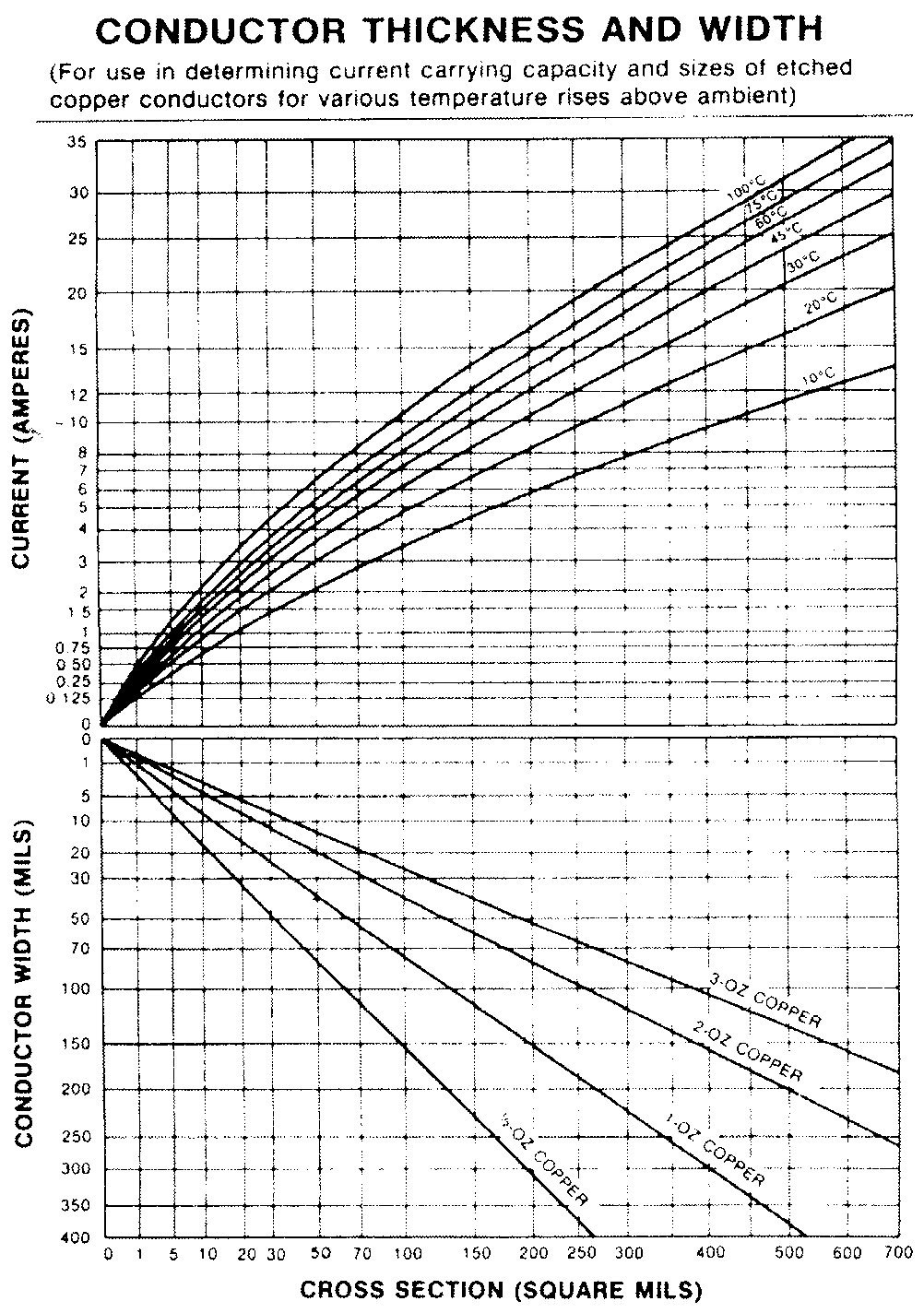
| Conductor and Thickness & Width Chart.pdf | 151.9 KiB | 2020-Mar-26 21:41 |
| Considerations on High-Speed Converter PCB Design Part 2 - Power & Ground Planes.pdf | 98.9 KiB | 2023-Jan-04 20:31 |
| Copper Foil Current Capacity Chart.jpg | 415.4 KiB | 2008-May-10 18:28 |
| Correct Board Layout Lowers EMI of Switchmode Converters - Maxim.mht | 361.0 KiB | 2011-Apr-10 21:21 |
| Crossing Split Plane Gaps.pdf | 101.2 KiB | 2010-May-30 16:21 |
| Design Issues.pdf | 1.9 MiB | 2020-Mar-11 15:23 |
| Designing Double Sided PCBs Part 2 in Pre CAD Days.pdf | 904.8 KiB | 2020-Mar-16 14:58 |
| Designing for Board Level EMC.pdf | 1.5 MiB | 2014-Sep-16 15:04 |
| Drill Size Equivalents.pdf | 62.8 KiB | 2020-Mar-26 21:38 |
| Dynamic Response Determination of an Electronic Printed Circuit Board - Nasa Tech Briefs.mht | 330.6 KiB | 2014-Sep-08 12:12 |
| ETI PCB Negatives Circa 1978.pdf | 132.2 KiB | 2009-Oct-04 00:16 |
| Electrical overstress in a nut shell.mht | 1.6 MiB | 2014-Jul-28 10:45 |
| Eliminating Ultrasonic Crosstalk.pdf | 73.7 KiB | 2009-Sep-19 21:14 |
| FPGA PCB Design and Pin Planning Guide.pdf | 2.9 MiB | 2015-May-26 12:13 |
| Fabrication.pdf | 61.5 KiB | 2020-Mar-26 21:37 |
| Flex CIrcuit Design.pdf | 542.9 KiB | 2010-Jun-13 21:13 |
| Flexible PCB Design Manual.pdf | 3.0 MiB | 2014-Oct-09 14:18 |
| Fly-Buck converter PCB layout tips - Power House - Blogs - TI E2E Community.mht | 1.8 MiB | 2016-Apr-05 11:24 |
| Ground Rules For High Speed Circuits.pdf | 356.8 KiB | 2006-Jan-27 16:16 |
| Grounding of Mixed Signal PCBs.pdf | 64.7 KiB | 2020-Mar-26 21:31 |
| Guidelines for 0.4mm Package-On-Package Packages Part 1.pdf | 6.5 MiB | 2015-May-26 12:11 |
| Guidelines for PCB Manufacturability.pdf | 130.9 KiB | 2015-Apr-30 17:56 |
| High Density PCB Layout of DC-DC Converters, Part 1 - Power House - Blogs - TI E2E Community.mht | 1.8 MiB | 2016-Apr-05 11:24 |
| High Speed Printed CIrcuit Board Layout.pdf | 470.0 KiB | 2020-Feb-02 01:49 |
| Highly Reliable Via In Pad Design February 2013.pdf | 245.8 KiB | 2015-May-26 11:26 |
| How to extract PCB CAD data.pdf | 89.6 KiB | 2011-Nov-28 18:01 |
| How to layout a PCB for an op amp - Precision Hub - Blogs - TI E2E Community.mht | 1.8 MiB | 2016-Jan-18 11:59 |
| Inductance In Between Spaces.pdf | 222.2 KiB | 2010-Jan-07 00:40 |
| Keeping Noise Out Of Your Designs.pdf | 589.2 KiB | 2009-Dec-05 22:27 |
| Laminated Bus Strips Ease PCB Layout.pdf | 130.6 KiB | 2009-Aug-29 22:07 |
| Laminates.pdf | 69.2 KiB | 2020-Mar-26 21:35 |
| Layout Rules.mht | 210.0 KiB | 2015-Aug-20 16:47 |
| Low Cost PCB Shields.pdf | 127.4 KiB | 2010-Jun-08 00:21 |
| MAXIMIZE POWER AND EFFICIENCY IN PCB PLACEMENT AND ROUTING.pdf | 874.8 KiB | 2014-Jun-13 11:18 |
| METRIC PITCH BGA AND MICRO BGA ROUTING SOLUTIONS.pdf | 669.5 KiB | 2014-Jun-13 11:18 |
| Make Your Pcb Design Ideas Fly High with Eagle.pdf | 268.1 KiB | 2023-Jun-13 23:18 |
| Marking Diodes - Vias in Pads.mht | 2.4 MiB | 2015-May-26 11:31 |
| Microvias, Blind and Buried Vias.mht | 612.7 KiB | 2015-May-26 11:34 |
| Minimize Noise in Audio Channels with Smart PCB Layout.mht | 406.1 KiB | 2011-Apr-10 21:58 |
| Multilayer PCB Designing Part 2 Electromagnetic Compatibility EFY 2016-08.pdf | 426.9 KiB | 2021-Apr-02 18:07 |
| OVERCOME THE CHALLENGES OF HIGHLY CONSTRAINED PCB DESIGNS.pdf | 710.4 KiB | 2014-Jun-13 11:06 |
| Optimum-PCB-Design-Handbook.pdf | 1.9 MiB | 2018-Mar-26 19:04 |
| PCB Design - Crosstalk in differential vias with Grounds.pdf | 110.2 KiB | 2021-Jul-12 18:08 |
| PCB Design - Problems with traces across split planes.pdf | 146.2 KiB | 2022-Apr-13 20:13 |
| PCB Design Issues for Op-Amps.pdf | 281.8 KiB | 2023-Dec-24 19:30 |
| PCB Layout Considerations for Non-Isolated Switching Power Supplies.pdf | 210.2 KiB | 2016-May-04 18:02 |
| PCB Layout Guidelines.mht | 269.3 KiB | 2015-Sep-11 13:00 |
| PCB Layout Techniques to Achieve RF Immunity for Audio Amplifiers.mht | 392.3 KiB | 2011-Apr-10 21:53 |
| PCB Layout for Schottky TTL.pdf | 806.1 KiB | 2009-May-23 00:36 |
| PCB Material Issues and Changing vendors.pdf | 377.8 KiB | 2020-Aug-23 18:16 |
| PCB Stack-Up - Part 1 Introduction.mht | 7.9 KiB | 2015-Jul-02 17:05 |
| PCB Stack-Up - Part 2.mht | 12.5 KiB | 2015-Jul-02 17:06 |
| PCB Stack-Up - Part 3.mht | 8.2 KiB | 2015-Jul-02 17:06 |
| PCB Stack-Up - Part 4.mht | 10.3 KiB | 2015-Jul-02 17:06 |
| PCB Stack-Up - Part 5.mht | 12.4 KiB | 2015-Jul-02 17:06 |
| PCB Stack-Up - Part 6 Return Path Discontinuities.mht | 95.6 KiB | 2015-Jul-02 17:05 |
| PCB layout considerations for nonisolated switching power supplies.pdf | 1.0 MiB | 2022-Nov-09 15:32 |
| PCB layout guidelines for gigasample ADCs.pdf | 954.3 KiB | 2021-Aug-10 19:27 |
| PHYSICAL DESIGN REUSE IN PCB DESIGN.pdf | 827.9 KiB | 2014-Jun-13 11:07 |
| Pads In That Via.mht | 697.4 KiB | 2015-May-26 11:33 |
| Partioning and Layout of a Mixed Signal PCB.pdf | 988.4 KiB | 2006-Oct-09 13:44 |
| Passives and Via In Pad.mht | 612.3 KiB | 2015-May-26 11:33 |
| Pcb Layout Information For Minimum Emi.pdf | 97.2 KiB | 2005-Nov-13 20:38 |
| Power and Ground Design.pdf | 95.3 KiB | 2010-Jan-11 23:55 |
| PowerPCB Quick Reference Card.pdf | 465.7 KiB | 2009-Oct-03 23:38 |
| Precautions on PCB Design.pdf | 120.9 KiB | 2011-Jun-10 22:49 |
| Printed Circuit Board Layout Guidelines.doc | 1.5 MiB | 2020-Jan-13 17:53 |
| Printed Circuit Board Layout Guidelines.pdf | 2.1 MiB | 2020-Jan-13 17:53 |
| Printed Electronic Circuitry and Components.pdf | 498.3 KiB | 2009-Apr-19 18:23 |
| Proper Layout and Component Selection Controls EMI - Maxim.mht | 413.2 KiB | 2011-Apr-10 21:14 |
| Proper PC-board layout to improve dynamic range.pdf | 544.4 KiB | 2020-Aug-06 23:30 |
| Proper PCB Layout Improves Dynamic Range.pdf | 2.0 MiB | 2020-Jun-12 15:20 |
| Protel99SE_PCB_ASCII_File_Format.pdf | 163.7 KiB | 2011-Nov-28 18:10 |
| RF and MICROWAVE Design Challenges in PCBs.pdf | 209.3 KiB | 2014-Jun-13 11:17 |
| Reducing crosstalk of an op amp on a PCB.pdf | 179.7 KiB | 2010-Jan-24 20:54 |
| Rigid-Flex Technology - Mainstream Use but More Complex Designs.pdf | 43.1 KiB | 2008-Mar-24 17:20 |
| Rigid-flex Design Guide.pdf | 150.4 KiB | 2008-Mar-24 17:19 |
| SAR ADC PCB Layout The reference path - Precision Hub - Blogs - TI E2E Community_aspx.mht | 1.6 MiB | 2014-Aug-25 11:06 |
| SILKSCREEN TIPS.pdf | 903.0 KiB | 2014-Nov-26 12:28 |
| SIX PRINCIPLES OF EASY-TO-USE PCB DESIGN CREATION.pdf | 626.7 KiB | 2015-Feb-04 12:10 |
| SMD Packaging Thermal Considerations.pdf | 1.0 MiB | 2001-Nov-16 11:00 |
| SOLDER PAD RECOMMENDATIONS FOR SMT Devices.pdf | 91.5 KiB | 2004-Aug-02 14:03 |
| Should You Use Your Power Plane as a Return Path_ _ PCB Design Blog _ Altium Designer.pdf | 966.3 KiB | 2020-Apr-08 18:45 |
| Solve High Speed PCB Design Challenges.pdf | 1.6 MiB | 2016-Sep-19 18:11 |
| THE SIX THINGS YOU WANT TO HAVE IN YOUR PCB DESIGN LIBRARY.pdf | 601.0 KiB | 2015-Mar-19 11:20 |
| THE UNIVERSAL PCB DESIGN GRID SYSTEM.pdf | 509.0 KiB | 2014-Jun-13 11:10 |
| Take Command of Thermal Optimization During PCB Design.pdf | 990.4 KiB | 2016-Mar-22 11:39 |
| The Engineer’s Guide To High-Quality PCB Design Embedded content from Electronic Design.mht | 2.2 MiB | 2016-Apr-05 11:20 |
| The Problem Of Adc And Mixed-Signal Grounding And Layout For Dynamic Performance While Minimizing Rfi-Emi.pdf | 277.3 KiB | 2004-Nov-04 12:04 |
| Three Challenges Impacting the Efficiency of PCB Engineering Teams.pdf | 1.5 MiB | 2014-Oct-09 17:04 |
| Tips For BGA Escape Routing.mht | 795.7 KiB | 2015-May-26 12:15 |
| Tips, hints for PCB Via Design.mht | 619.4 KiB | 2015-May-26 12:12 |
| Tolerances.pdf | 200.6 KiB | 2020-Mar-26 21:43 |
| Trace Spacing Calculation for Voltage Levels.mht | 425.8 KiB | 2015-May-29 15:12 |
| Transmission Lines Initial Conditions.pdf | 84.6 KiB | 2009-Feb-12 23:41 |
| USING HYPERLYNX DRC TO FIND EMI ISSUES.pdf | 1.1 MiB | 2014-Oct-21 15:01 |
| Via in Pad Hints.mht | 277.1 KiB | 2015-May-26 11:30 |
| Via in Pad.mht | 556.4 KiB | 2015-May-26 11:22 |
| Via-in-Pad Blind Via Technology.pdf | 569.0 KiB | 2015-May-26 11:36 |
| Vibration Stress Analysis.pdf | 257.4 KiB | 2009-May-22 23:37 |
| Wide Band Amplifier PCB Design Issue.pdf | 184.6 KiB | 2010-Aug-23 22:36 |